Smartphone Camera Sensors Explained
Today’s smartphones are so powerful that they could’ve not only launched all the Apollo missions to the Moon but also taken all the photos and videos from the Moon’s surface and posted them on Instagram.
All jokes aside, the technology behind modern smartphone cameras is so advanced, from the sensors to all the software algorithms, that one can use a smartphone to capture images and video for pretty much every imaginable scenario.
There’s a comprehensive list of movies shot entirely on smartphones, and many photography exhibitions and contests also rely on the smartphone as a primary tool of choice. These exhibitions not only feature some pretty popular names in the industry, but the exhibits are quite astonishing.
What sits behind all this? What makes smartphones good enough, even for professional photographers and filmmakers? What is a CMOS sensor, and what exactly is a double-layer transistor-pixel design? Today we’re going to answer these questions.
A brief history of the camera phone
The first commercial camera phone
We’re not going to bore you with many historical details, but just for context, the first patent for a camera phone dates back to 1994, when four Nokia employees decided to create a phone with an integrated camera inside.
Funnily enough, the first camera phone was not made by Nokia. It was a Japanese Kyocera VP-210, dubbed Visual Phone, released in May 1999. For the 25 years that followed, things moved rapidly, and now we have 1-inch smartphone sensors, stacked sensors, dual-layer transistor-pixel designs, and more.
But what hasn’t changed is the basic technology that captures light and turns it into an electrical signal to store it in your phone’s memory or display it on the screen.
What is a CMOS sensor?
Active-pixel sensor, image courtesy of Wikipedia
This technology was invented way back in 1968, and the abbreviation stands for Complementary Metal-Oxide Semiconductor. It’s not as complicated as it sounds. There are photodiodes that catch the light and turn it into an electrical signal, and then there are transistors that amplify that signal.
These are also called APS, or active-pixel sensors, because each photodiode has a separate transistor that actively amplifies the signal. So we have a lens focusing the light, a photodiode capturing the photons from the light and converting them to electrons or electrical signals, and transistors amplifying that signal and sending it to the ISP (image signal processing) chip for further processing.
The first CMOS design was problematic
So far, so good. The early CMOS sensors had their metal circuitry between the photodiode and the lens, obstructing the light and making the image darker. These were known as FSI (front-side illumination) sensors.
The next generation of CMOS sensors moved the photodiode above the wiring and next to the lens, capturing the light, thus allowing more light to be captured by the diode. This design is known as BSI (back-side illumination). One of the first phones to feature this type of sensor was the iPhone 4.
Invention of the stacked CMOS sensor
Around 2008, Taku Umebayashi, who was an engineer at Sony Semiconductor Solutions Corporation, decided he could improve this design and started working on a stacked CMOS sensor.
The idea was to completely separate the circuit section from the photodiode. Prior to that, the circuit was wrapped around the photodiode, taking up precious space and forcing the photodiode to be smaller in size. The smaller the photodiode, the less light it can capture, resulting in reduced low-light sensitivity and also more noise from the circuit around it.
The first stacked CMOS design was pioneered by Sony
The first commercially available stacked CMOS sensor was introduced by Sony back in 2012, and it revolutionized digital photography. Umebayashi received the 2016 National Invention Award from the Prime Minister of Japan and the 2020 Medal with Purple Ribbon Award for his invention.
Plaques of the Prime Minister’s Award (2016 National Invention Awards) and 2020 decoration of the Medal with Purple Ribbon
Another fun fact is that at the time the stacked CMOS sensor entered mass production, there were literally zero clients for the technology. It was a huge gamble, and Sony decided to put the stacked CMOS sensor in its Xperia Z line of smartphones in order to popularize it.
This gamble paid off. Not long after the launch of the stacked CMOS, smartphone manufacturers recognized the superiority of the technology, and nowadays most smartphones (including all the iPhones) feature Sony image sensors. Sony is the absolute leader in market share when it comes to CMOS sensors, with a whopping 42% (data from 2022), with Samsung a distant second with 19%.
The dual-layer transistor-pixel design
Another buzzword, or should we say buzzphrase, was coined last year, and that’s the dual-layer transistor-pixel mobile sensor. The stacked CMOS sensors were good, but the transistor part amplifying the signal was still a part of the photodiode, limiting the surface that captures light.
In 2021, Sony Semiconductors announced another breakthrough in the CMOS field. It’s the world’s first 2-layer transistor-pixel CMOS sensor. The engineers found a way to move the transistor part, amplifying the signal under the photodiode, leaving more surface for capturing light, and improving thins such as dynamic range, low light sensitivity, and lowering the noise.
2-layer transistor-pixel stacked sensor design, Sony
Here’s an excerpt from Sony’s site explaining the tech: “The 2-Layer Transistor Pixel is the world’s first stacked CMOS image sensor technology with a pixel structure that separates photodiodes and pixel transistors on different substrate layers, as opposed to the conventional style of having the two on the same substrate. This new structure approximately doubles saturation signal level relative to conventional image sensors, widens dynamic range, and reduces noise.”
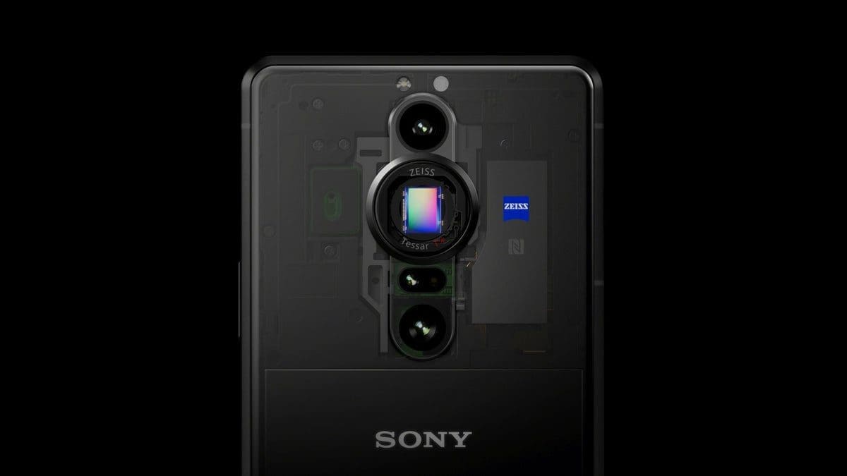
The technology made its way to the Sony Xperia 1 Mark V (dubbed Exmor T) and subsequently to many other flagship phones (Xiaomi 14 series, OnePlus 12) under the rebranded Sony LYTIA sensors lineup.
Conclusion
As the experts in the field of digital photography say, “the future is stacked!” This means that in the years to come, we will see this technology inside more and more flagship (and midrange) phones. What comes next? Only time will tell!


