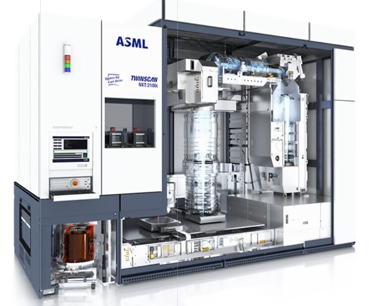
Those in the know say that the controversial application processor (AP) was produced using a deep ultraviolet lithography (DVL) machine to etch the circuitry patterns on the silicon wafers that the chips were built on before getting sliced into individual dies. Because each chip contains billions of transistors, the lithography equipment is used to create patterns that are thinner than human hair. Tools from other companies were also used to manufacture the chip according to the report.
The DUV machine is not the most advanced technology in this area as ASML’s extreme ultraviolet lithography (EUV) machines are used to produce chips with a 7nm or lower process node. ASML is the only company in the world producing the EUV machines and it does not ship them to China.

One of the Deep Ultraviolet Lithography machines sold by ASML
DUVs have been shipped to China but last summer the Biden administration pressured ASML to announce that it won’t ship three out of four of its second most advanced DUV lithography machines to China without a license. But that restriction doesn’t start until January which means that there was nothing that could have prevented SMIC from using the machine to produce the Kirin 9000s.
The rule used by the Biden administration to block shipments of ASML’s machines to China is called a de minimis rule which allows the U.S. to control the export of lithography machines that contain U.S. technology. It is the same rule used by the U.S. to prevent foundries using American technology to produce chips from shipping advanced silicon to Huawei without a license.
Huawei did obtain a license that allowed it to use a 4G version of Qualcomm’s 4nm Snapdragon 8+ Gen 1 AP to power the Mate 50 flagship series in 2022, and the P60 flagship series earlier this year. The use of the 7nm Kirin 9000s, which does support 5G, to run the Mate 60 flagship line shocked and stunned the smartphone world while exciting consumers in China.


